
MagiCache: A Virtual In-Cache Computing Engine
Compute directly in your cache

MagiCache: A Virtual In-Cache Computing Engine Renhao Fan, Yikai Cui, Weike Li, Mingyu Wang, and Zhaolin Li ISCA'25
This paper presents an implementation of RISC-V vector extensions where all vector computation occurs in the cache (i.e., SRAM-based in-memory computation). It contains an accessible description of in-SRAM computation, and some novel extensions.
Compute in SRAM
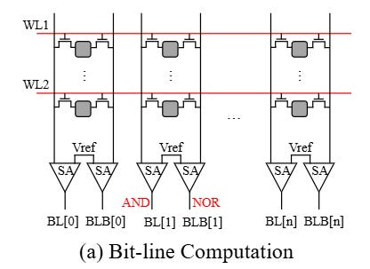
Recall that SRAM is organized as a 2D array of bits. Each row represents a word, and each column represents a single bit location in many words. A traditional read operation occurs by activating a single row. Analog values are read out from each bit and placed onto shared bit lines. There are two bit lines per column (one holding the value, one holding the complement). Values flow down to sense amplifiers that output digital values.
Prior work has shown that this basic structure can be augmented to perform computation. Rather than activating a single row, two rows are activated simultaneously (let’s call the values of these rows A and B). The shared bit lines perform computation in the analog domain, which results in two expressions appearing on the output of the sense amplifiers: (A AND B) and (A NOR B). Fig. 1(a) shows a diagram of such an SRAM array:
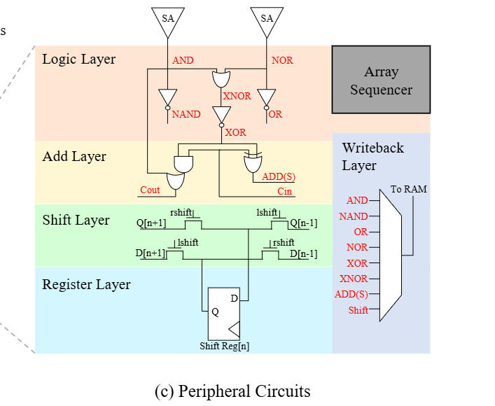
If you slap some digital logic at the end of the sense amplifiers, then you can generate other functions like OR, XOR, XNOR, NAND, shift, add. Shift and add involve horizontal connections. Fig. 4(c) shows a hardware diagram of this additional logic at the end of the sense amplifiers. Note that the resulting value can be written back into the SRAM array for future use. Multiplication is not directly supported but can be implemented with a sequence of shift and add operations.
Virtual Engine
The innovation in this paper is to dynamically share a fixed amount of on-chip SRAM for two separate purposes: caching and a vector register file. The logical vector register file capacity required for a particular algorithm depends on the number of architectural registers used, and the width of each architectural register (RISC-V vector extensions allow software to configure a logical vector width). Note that this hardware does not have separate vector ALUs, the computation is performed directly in the SRAM arrays.
Fig. 6 illustrates how the hardware dynamically allocates SRAM space between generic cache storage and vector registers (with in-memory compute). The unit of allocation is a segment. The width of a vector register determines how many segments it requires.
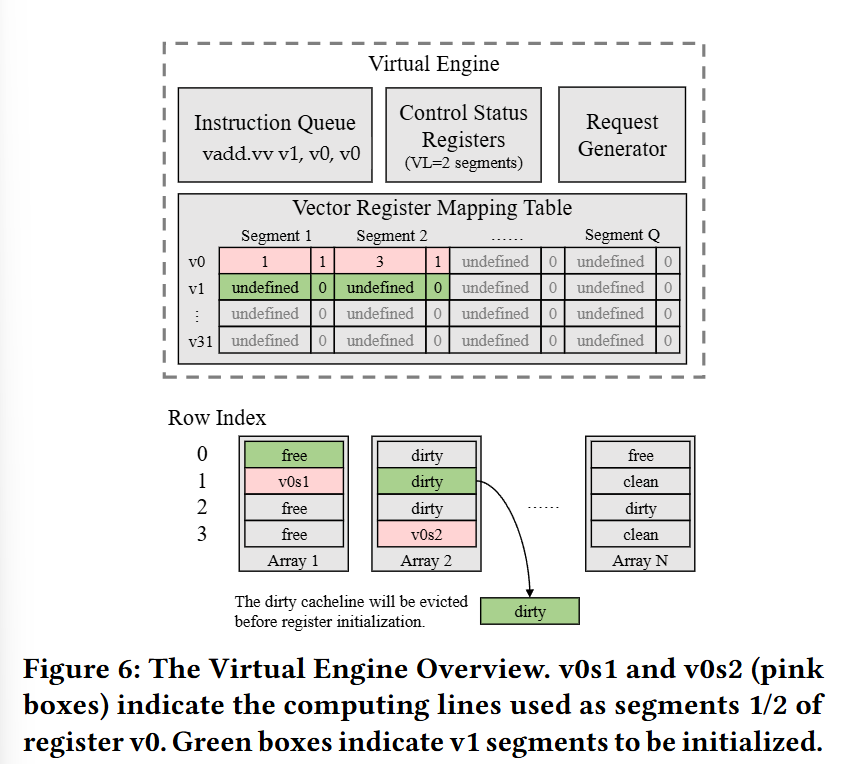
Initially, all SRAM space is dedicated to caching. When the hardware processes an instruction that writes to an uninitialized vector register, then the hardware allocates segments to hold data for that register (evicting cached data if necessary). This system assumes an enlightened compiler which will emit a vsetvli instruction to hint to the hardware when it has reached a point in the instruction stream where no vector register has valid content. The hardware can use this hint to reallocate all memory back to being used for caching.
Results
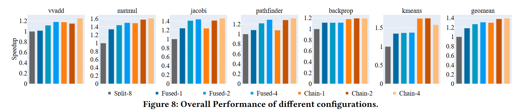
Fig. 8 shows performance results normalized against prior work (labeled Split-8 here). This shows a 20%-60% performance improvement, which is pretty good considering that the baseline offers an order-of-magnitude improvement over a standard in-order vector processor.
Dangling Pointers
I wonder how this would compare to hardware that did not have a cache, but rather a scratchpad with support for in-memory computing.